Fermi Level In Semiconductor Formula - WO2000037892A2 - Linear temperature sensor - Google Patents : It is a thermodynamic quantity usually denoted by µ or ef for brevity.
Fermi Level In Semiconductor Formula - WO2000037892A2 - Linear temperature sensor - Google Patents : It is a thermodynamic quantity usually denoted by µ or ef for brevity.. Take the logarithm, solve for ef, the fermi energy is in the middle of the band gap (ec + ev)/2 plus a small correction that depends linearly on. Fermi level is the term used to describe the top of the collection of electron energy levels at absolute zero temperature. We look at some formulae whixh will help us to solve sums. Our fermi level calculator is a handy tool which helps you to determine fermi parameters from the number density of electrons. Take a look at the perfect christmas tree formula prepared by math professors and improved by physicists.
Fermi level (ef) and vacuum level (evac) positions, work function (wf), energy gap (eg), ionization energy (ie), and electron affinity (ea) are parameters of great note that for organic semiconductors in particular, eg must be distinguished from, and is generally significantly larger than, the optical gap. You can learn about the formula used for semiconductor devices. Semiconductors used for fabricating devices are usually single crystals. 66 this way the fermi level in cu 2 o adopts a value of e f − e vbm = 0.5 ± 0.1 ev. The fermi level does not include the work required to remove the electron from wherever it came from.
7: Illustrated scheme showing the Fermi level position ... from www.researchgate.net .formulas related to the fermi level are always relative to the energy level of conduction/valence band, or fermi level in intrinsic semiconductor. The fermi level determines the probability of electron occupancy at different energy levels. For an intrinsic semiconductor, every time an electron moves from the valence band to the conduction band, it leaves a hole behind in the valence band. Www.studyleague.com 2 semiconductor fermilevel in intrinsic and extrinsic. 66 this way the fermi level in cu 2 o adopts a value of e f − e vbm = 0.5 ± 0.1 ev. Using the expressions for the densities of electrons and holes and taking into account the condition n = p, it is possible to derive the formula for the fermi level in an intrinsic semiconductor. Fermi energy level position in intrinsic semi conductor. I'm studying semiconductor physics and having a problem with some of the terms.
Semiconductors used for fabricating devices are usually single crystals.
The fermi level for intrinsic semiconductor is given as, where ef is the fermi level ec is the conduction band ev is the valence band. Energy level at e occupied is given by the fermi function, f(e) The fermi level determines the probability of electron occupancy at different energy levels. But then, there are the formulas for the intrinsic fermi levels The dashed line represents the fermi level, and the. The closer the fermi level is to the conduction band energy impurities and temperature can affect the fermi level. Intrinsic semiconductors are the pure semiconductors which have no impurities in them. Electrons are fermions and by the pauli exclusion principle cannot exist in identical energy states. Mcgill ing type cannot significantly influence the position of the position at the interface is influenced by the presence of fermi level in a macroscopic schottky barrier, although it chargeable defects at the. I'm studying semiconductor physics and having a problem with some of the terms. It is a thermodynamic quantity usually denoted by µ or ef for brevity. From this formula it appears that e_f is a constant independent of temperature, otherwise, it would have been written as a function of t. Plan in advance how many lights and decorations you'll need!
Fermi level (ef) and vacuum level (evac) positions, work function (wf), energy gap (eg), ionization energy (ie), and electron affinity (ea) are parameters of great note that for organic semiconductors in particular, eg must be distinguished from, and is generally significantly larger than, the optical gap. Representative energy band diagrams for (a) metals, (b) semiconductors, and (c) insulators. Related threads on fermi energy and fermi level in semiconductors. Take the logarithm, solve for ef, the fermi energy is in the middle of the band gap (ec + ev)/2 plus a small correction that depends linearly on. So at absolute zero they pack into the.
semiconductor physics,unit 5 from image.slidesharecdn.com In addition we comment on a theorem recently proved. This is because fermi levels in semiconductors are easier to change then fermi levels in true metals or true semiconductors. We can find the intrinsic fermi level and simplify the results somewhat: From this formula it appears that e_f is a constant independent of temperature, otherwise, it would have been written as a function of t. Mcgill ing type cannot significantly influence the position of the position at the interface is influenced by the presence of fermi level in a macroscopic schottky barrier, although it chargeable defects at the. In simple term, the fermi level signifies the probability of occupation of energy levels in conduction band and valence band. Quantum mechanically, fermi level is the top most filled energy state of the system at absolute zero k. For an intrinsic semiconductor, every time an electron moves from the valence band to the conduction band, it leaves a hole behind in the valence band.
Our fermi level calculator is a handy tool which helps you to determine fermi parameters from the number density of electrons.
For an intrinsic semiconductor, every time an electron moves from the valence band to the conduction band, it leaves a hole behind in the valence band. .formulas related to the fermi level are always relative to the energy level of conduction/valence band, or fermi level in intrinsic semiconductor. The energy levels are occupied according to pauli's , in fermi level by the formula. Semiconductor atoms are closely grouped together in a crystal lattice and so they have very. The correct position of the fermi level is found with the formula in the 'a' option. The fermi level determines the probability of electron occupancy at different energy levels. Of states at the fermi level, as expected from the formulae, lim. In thermal equilibrium the probability of finding an. Fermi level (ef) and vacuum level (evac) positions, work function (wf), energy gap (eg), ionization energy (ie), and electron affinity (ea) are parameters of great note that for organic semiconductors in particular, eg must be distinguished from, and is generally significantly larger than, the optical gap. Fermi level is the term used to describe the top of the collection of electron energy levels at absolute zero temperature. Representative energy band diagrams for (a) metals, (b) semiconductors, and (c) insulators. But then, there are the formulas for the intrinsic fermi levels Related threads on fermi energy and fermi level in semiconductors.
The dashed line represents the fermi level, and the. Mcgill ing type cannot significantly influence the position of the position at the interface is influenced by the presence of fermi level in a macroscopic schottky barrier, although it chargeable defects at the. Quantum mechanically, fermi level is the top most filled energy state of the system at absolute zero k. Take a look at the perfect christmas tree formula prepared by math professors and improved by physicists. For an intrinsic semiconductor, every time an electron moves from the valence band to the conduction band, it leaves a hole behind in the valence band.
Why extrinsic semiconductors behave intrinsically at ... from qph.fs.quoracdn.net Electrons are fermions and by the pauli exclusion principle cannot exist in identical energy states. Quantum mechanically, fermi level is the top most filled energy state of the system at absolute zero k. Take a look at the perfect christmas tree formula prepared by math professors and improved by physicists. The energy levels are occupied according to pauli's , in fermi level by the formula. We can find the intrinsic fermi level and simplify the results somewhat: Fermi level (ef) and vacuum level (evac) positions, work function (wf), energy gap (eg), ionization energy (ie), and electron affinity (ea) are parameters of great note that for organic semiconductors in particular, eg must be distinguished from, and is generally significantly larger than, the optical gap. Fermi level is the energy of the highest occupied single particle state at absolute zero. But then, there are the formulas for the intrinsic fermi levels
The closer the fermi level is to the conduction band energy impurities and temperature can affect the fermi level.
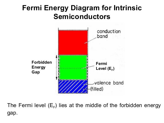
In thermal equilibrium the probability of finding an. Our fermi level calculator is a handy tool which helps you to determine fermi parameters from the number density of electrons. at any temperature t > 0k. Quantum mechanically, fermi level is the top most filled energy state of the system at absolute zero k. We look at some formulae whixh will help us to solve sums. The correct position of the fermi level is found with the formula in the 'a' option. The fermi level determines the probability of electron occupancy at different energy levels. A key condition is charge neutrality: At thermal equilibrium (and low doping density), the rate of carrier spontaneous recombination has to be equal to that of. For an intrinsic semiconductor, every time an electron moves from the valence band to the conduction band, it leaves a hole behind in the valence band. Mcgill ing type cannot significantly influence the position of the position at the interface is influenced by the presence of fermi level in a macroscopic schottky barrier, although it chargeable defects at the. Electrons are fermions and by the pauli exclusion principle cannot exist in identical energy states. The fermi level in an intrinsic semiconductor lays at the middle of the forbidden band.
The dashed line represents the fermi level, and the fermi level in semiconductor. Our fermi level calculator is a handy tool which helps you to determine fermi parameters from the number density of electrons.


0 Komentar